Applications
Semiconductor.
Packages and solder joints.
Inspection tasks
See every solder joint.
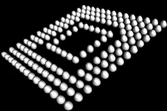
Packages hide their connections under the die and the mould compound. X-ray and CT show voids, bridges and misalignment joint by joint, for the laboratory and for the line.
BGA and flip-chip joints
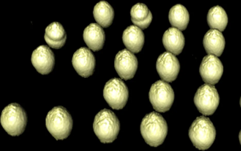
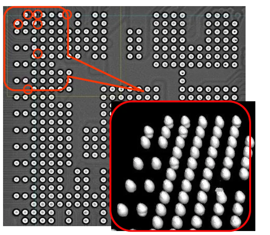
Voids, solder-ball shift, head-in-pillow defects and bridges are separated layer by layer. Planar CT does this on the full board, without cutting it.
Leads and bond wires
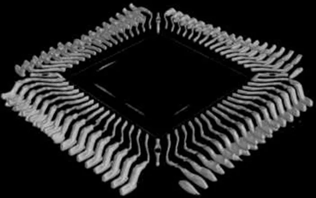
Lifted or bent leads, open joints and bond-wire defects show in the 3D volume, where a 2D image superimposes them.
Failure analysis
Micro-cracks, micro-voids and delamination are located before the cross-section is made, so the cut goes through the right place.
Scan examples
What the data shows.