
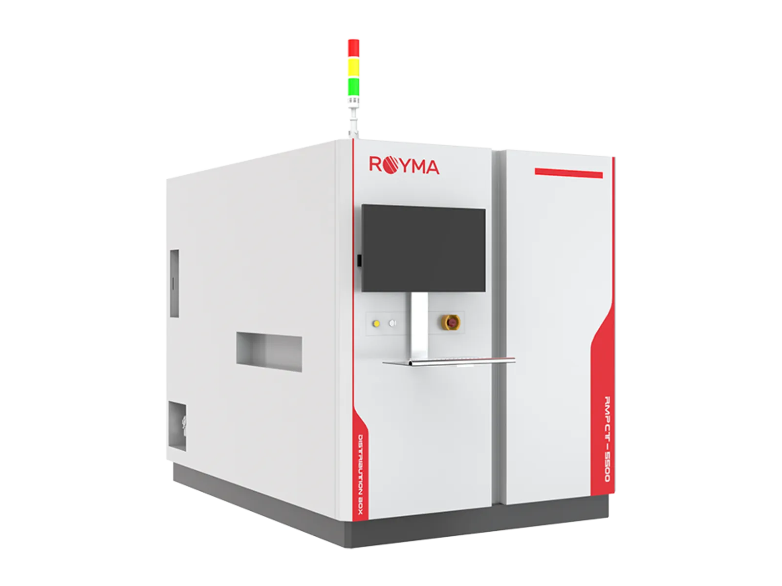
- Per field of view, fastest setting
- 2 s
- Resolution, selectable
- 3–30 µm
- Board size, up to, by configuration
- 760 × 660 mm
- CT slices per scan
- > 300
Overview
Layer by layer. Without cutting.
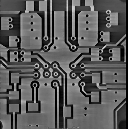
A 2D X-ray image overlays every layer of a printed circuit board (PCB). A cross-section shows one plane and destroys the board. Planar computed tomography (CT) separates the layers and leaves the board intact.
The RMPCT5500 inspects assembled boards in the line or beside it. It measures solder joints, voids, back-drilled stubs and layer spacing, and marks each feature OK or not OK.
Planar CT is made for flat assemblies. Thick, three-dimensional parts need a system with a rotating sample or gantry.
Features
From image to decision.
Three imaging modes
Use as much depth as the task needs. 2D, 2.5D and 3D planar CT run on one system, with projection angles of 30° or 45° and up to 1024 projections.
Measure what was hidden
Replace the cross-section. The software measures back-drilled stub depth, residual copper height, layer spacing and hole eccentricity against your limits.
Judge automatically
Remove manual thresholds. Defect regions are found and judged OK or not OK automatically; void ratio and solder fill are reported per joint.
Program from CAD
Change products quickly. Inspection programs are generated from CAD data.
Keep every result
Trace each board. Results are exported to your manufacturing execution system (MES).
Inline or at-line
Place it where it helps. The system loads boards automatically with a pneumatic clamp and works in the line or as a stand-alone station.
Specifications
Technical data.
| Imaging | |
|---|---|
| Modes | 2D, 2.5D, 3D planar CT |
| Projection angles | 30° / 45° |
| Projections | 32 to 1024 |
| CT slices | More than 300 |
| Fastest inspection | 2 s per field of view |
| Resolution | 3–30 µm, selectable |
| X-ray source | |
| Tube voltage | 40–180 kV, by configuration |
| Tube current | 10–300 µA |
| Detector | |
| Flat panel | 49.5 µm pixels, 14 bit, up to 15 fps |
| Sample | |
| Board size | 600 × 660 mm or 760 × 660 mm, by configuration |
| Board thickness | 1–7 mm |
| Permitted warping | ± 2 mm |
| Installation | |
| Power | Single phase 220 V, 50/60 Hz, 5000 W |
| Weight | About 3 t |
| Radiation leakage | ≤ 1 µSv/h |
| Noise | ≤ 70 dB(A) |
Applications
Where it is used.
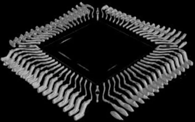
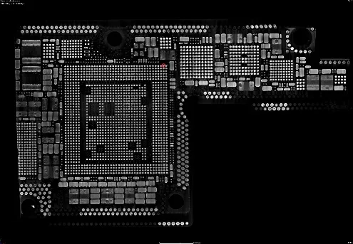
Solder voids, insufficient through-hole fill, back-drill stub depth, layer spacing and hole eccentricity in multilayer boards, backplanes and power substrates.
Downloads
Data sheet on request.
We send the current RMPCT5500 data sheet together with a first assessment of your part.