Application note ·
Royma RMPCT5500 brings inline planar CT to IC-substrate and advanced packaging lines
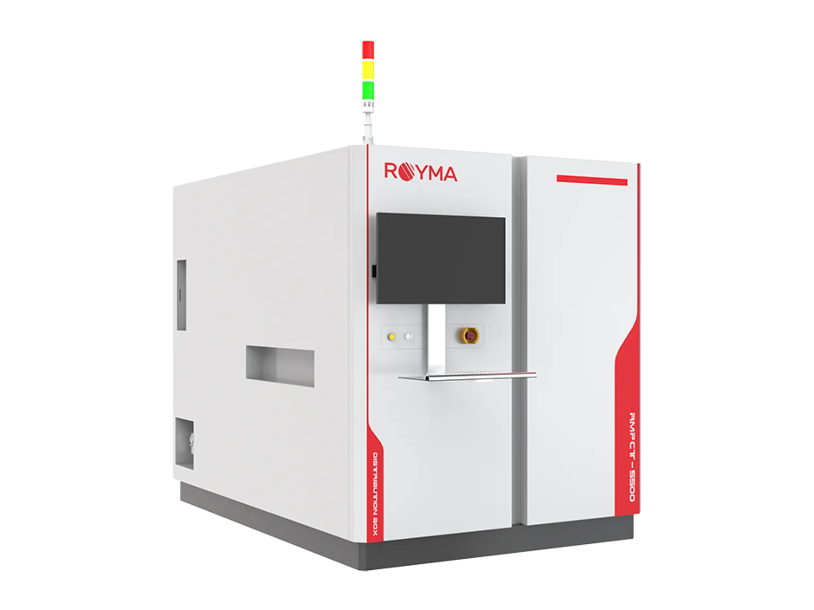
The Royma RMPCT5500 brings inline planar CT to IC-substrate and advanced packaging lines, combining 2D, 2.5D and 3D planar computed tomography (CT) in one machine with more than 300 CT slices per scan and a maximum inspection efficiency of 2 s per field of view. The RMPCT5500 separates the stacked interconnect levels of a package or substrate that overlap in a 2D X-ray image, so solder balls, lands and joints are checked in their own plane without sectioning the part.
- Imaging modes: 2D, 2.5D and 3D planar CT in one machine, chosen per inspection point
- Slicing: more than 300 CT slices, read in the XY, XZ and YZ directions from a chosen reference plane
- Speed: maximum inspection efficiency of 2 s per field of view
- Parts: substrates and boards 1–7 mm thick and up to 760 × 660 mm, with ±2 mm warp
- Integration: inline or at-line operation, synchronous AOI and MES connection
Stacked interconnects separated slice by slice
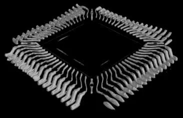
In a 2D X-ray image of a ball grid array, a chip-scale package or a multilayer substrate, joints on different levels project on top of one another. A cross-section resolves them, but it scraps the sample, shows a single plane and risks deformation from grinding and polishing. The RMPCT5500 replaces that step with planar CT: it views the part at projection angles of 30° or 45° and reconstructs the region of interest from 32 up to 1024 projections. The result is a stack of more than 300 slices that can be read in three directions, so each interconnect level is inspected on its own.
The RMPCT5500 is designed for the defects that a top-down projection hides: voids in solder balls and lands, pillow (head-in-pillow) joints, open and non-wetted joints, bridging, insufficient solder, shifted balls, lifted leads and foreign matter. It covers BGA, CSP, LGA, QFN and QFP packages as well as power modules and chip components. Resolution is selectable between 3 and 30 µm, so the setting follows the ball or land size of the part rather than one fixed magnification. “The RMPCT5500 shows each solder level of a package on its own slice, so a void or a pillow joint is no longer hidden behind the layer above it,” says Gabor Szabo, Sales Director Europe, Royma Europe.
Sized for substrates and boards on the line
The RMPCT5500 accepts substrates and boards from 1 to 7 mm thick and up to 760 × 660 mm, with a load of 3.5 kg as standard and up to 8 kg as an option. A pneumatic clamp holds the part by a 3 mm edge, and the machine accepts warp of ±2 mm. Before each scan, a laser measures the reference plane and compensates the warp at component level in 1 µm steps. An optical camera image is used to navigate and select the regions of interest; loading, scanning and unloading then run automatically.
The machine works as an inline station or at-line beside the production line, with synchronous AOI and MES integration that keeps every result traceable to its part. Its X-ray source operates from 40 to 180 kV at 10–300 µA and up to 40 W target power. A 14-bit flat-panel detector with 2304 × 2940 pixels and a 49.5 µm pixel size records the projections at up to 15 frames per second. The X-ray source moves in X, Y and Z and the detector in X and Y, which places the field of view on any point of the part.
Clean slices for automatic pass/fail judgement
The RMPCT5500 reconstructs with a super-resolution, artefact-suppressing algorithm, which keeps the slices clear enough for automatic evaluation. AI-based image recognition then judges each joint, and automated system calibration keeps the machine geometry consistent from scan to scan. The software quantifies the void ratio per solder land and the solder fill of through-hole joints, and returns a pass or fail result per joint to the MES. Because 2D, 2.5D and 3D planar CT run in the same machine, one inspection programme can combine fast 2D checks of uncritical areas with 3D planar CT on the joints that matter.
For a new package or substrate design, Royma sets the resolution, projection count and imaging mode on the customer’s own parts before the programme goes on the line. “We define the inspection programme on real substrates and packages, so resolution and cycle time are fixed against the parts the line will actually build,” adds Szabo. The same machine also inspects HDI boards and back-drilled vias, described in the application note on inline 3D planar CT for HDI boards. More applications are listed under semiconductor and consumer electronics.
| RMPCT5500 | Stated value |
|---|---|
| Imaging modes | 2D, 2.5D, 3D planar CT |
| Projection angles | 30° / 45° |
| Projections | 32 to 1024 |
| CT slices | more than 300 (XY, XZ, YZ) |
| Maximum inspection efficiency | 2 s per field of view |
| Resolution | 3–30 µm, selectable |
| Tube voltage / current | 40–180 kV / 10–300 µA |
| Target power | up to 40 W |
| Detector | 2304 × 2940 pixels, 14-bit, 49.5 µm pixel size, up to 15 fps |
| Maximum field of view | 57 × 73 mm |
| Substrate / board thickness | 1–7 mm |
| Maximum sample size | 760 × 660 mm |
| Load | 3.5 kg, optional up to 8 kg |
| Warp | ±2 mm |
| Operation | inline or at-line, synchronous AOI, MES integration |
Test scans available
Royma Europe offers test scans of customer substrates, packages and assemblies on the RMPCT5500. Contact Gabor Szabo, Sales Director Europe, Royma Europe, gabor_szabo@roymatek.eu, +49 15156503316 – www.roymatek.eu.
Royma Europe, Leibniz Universität Hannover – Institut für Produktentwicklung und Gerätebau, Gebäude 8143, An d. Universität 1, 30823 Garbsen, Germany.
About Royma: Royma Industrial CT develops and builds industrial X-ray and computed tomography systems, from 2D X-ray to horizontal, gantry, planar and inline CT.