Application note ·
Royma RMCT2000HR brings sub-micron CT to hybrid bonding void inspection
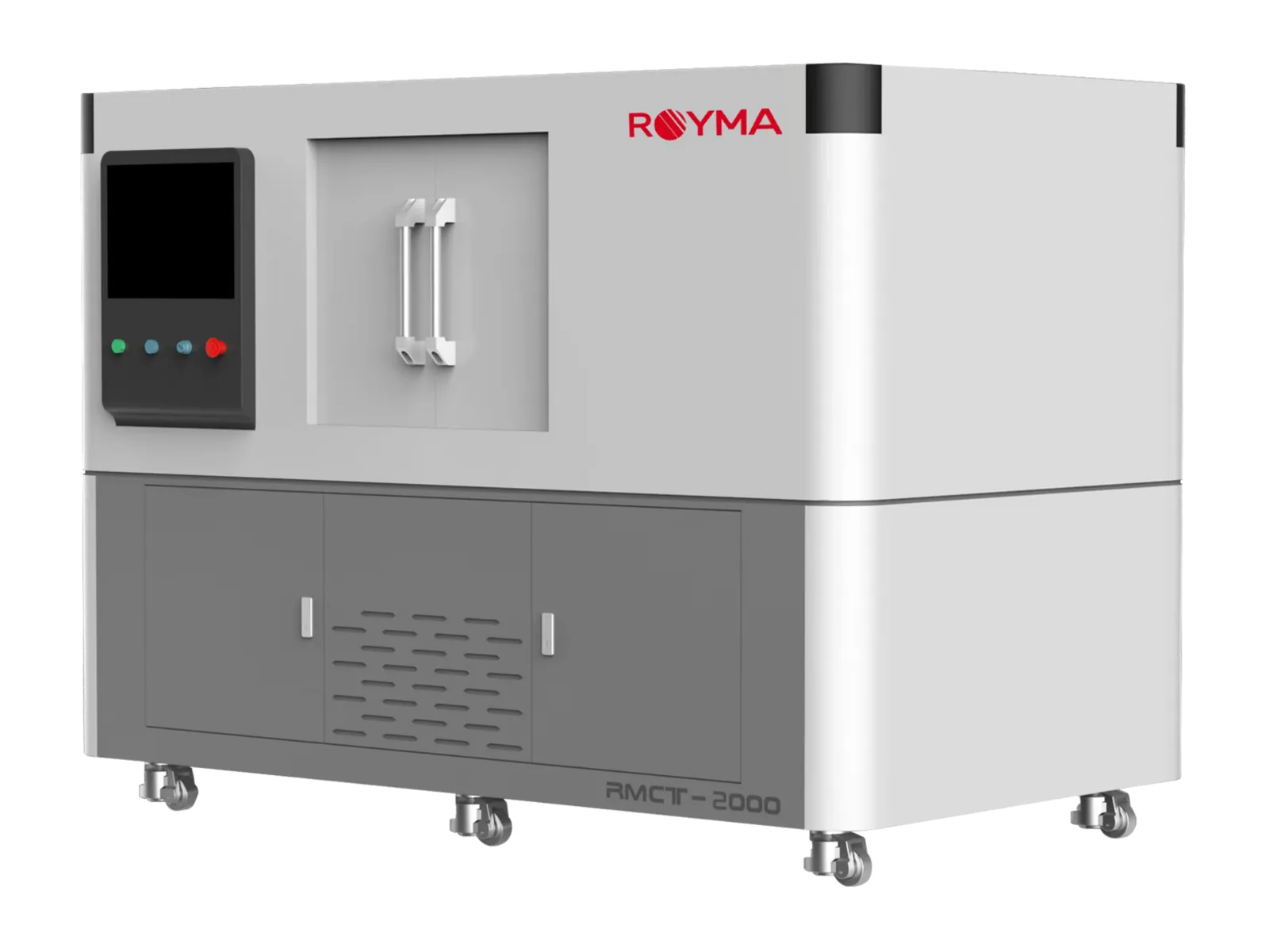
The Royma RMCT2000HR brings nanofocus computed tomography (CT) to hybrid bonding void inspection, with a stated 2D resolution of 0.5 µm (JIMA) and a 3D resolution of 1 µm. The open-tube nanofocus system images buried chiplet interfaces, micro-bumps and through-silicon vias in 3D, so bonding voids are located before a package is cross-sectioned.
Chiplet and hybrid-bonded stacks hide their joints between layers of silicon. A cross-section shows one plane of one sample and destroys it; a 2D X-ray image overlays every bond layer in a single projection. The RMCT2000HR replaces both with a volume that can be sliced along any bond layer after the scan.
Sub-micron CT for buried bond layers
The RMCT2000HR combines an open-tube nanofocus X-ray source of 110–190 kV with a CsI flat-panel detector of 3072 × 3072 pixels. At 190 kV and 25 W the source reaches a focal spot resolution of 0.5 µm on the JIMA chart. The system is built for small samples: parts up to 150 × 150 × 150 mm and 5 kg sit on the rotary table close to the source, where geometric magnification gives the finest voxel size.
For an advanced-packaging laboratory the machine covers the features that decide the yield of a bonded stack:
- Interface voids: unbonded areas and trapped gas between bonded dies or between die and interposer.
- Micro-bumps and solder joints: missing, bridged or voided bumps in a dense array.
- Through-silicon vias: incomplete fill and voids along the via.
- Delamination and micro-cracks: separation and cracking in the die, the bond line or the underfill.
A volume sliced along each bond layer
The RMCT2000HR scans the coupon or package once and reconstructs a 3D volume with a stated 3D resolution of 1 µm. From that volume the analyst extracts a virtual slice parallel to each bond interface. A void then appears in its true position and outline, without the overlay of the layers above and below it.
The same data set shows bumps, vias and the die stack in cross-section at any angle. Delamination and cracks are followed through the depth of the stack rather than judged from one cut face. Each slice is located against the package geometry, so a defect found by CT is cut open at the right place if a physical section is still wanted for confirmation.
The RMCT2000HR supports circular and helical scanning, segmented scanning for taller samples and a jitter scan mode that suppresses ring artefacts. Its stated measuring accuracy is 3.0 + L/50 µm, which allows bump height, bond-line thickness and void size to be measured in the volume, not only seen.
“The RMCT2000HR gives a packaging team a 3D view of every bond layer in a stack before anything is cut,” says Gabor Szabo, Sales Director Europe, Royma Europe. “Failure analysis starts from the volume, and the section goes exactly where the void is.”
What the data shows
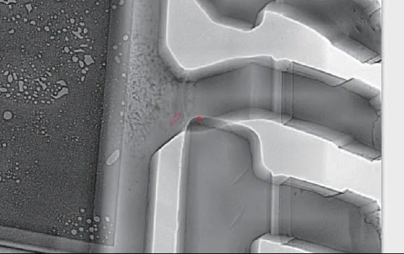
The picture above is a CT image of an electronic package: voids in the die-attach layer appear as bright, rounded spots on the left, while the lead-frame contacts on the right are rendered with their edges intact. Hybrid-bond interfaces are read in the same way. A void appears as a contrast change in the slice that runs along the bond layer, and its area is measured against the bonded area of the die.
Fine-pitch arrays benefit most from the 3D view. A micro-bump with a void at its root can look complete in a top-down 2D image because the bumps above and below overlap it. In the CT volume each bump is isolated, so voided, bridged and missing bumps are counted per die and per interposer site. Through-silicon vias are followed from top to bottom, and incomplete fill shows as a gap along the via axis.
Practical notes for bonded stacks
Sample size decides the achievable voxel size. The closer a sample sits to the nanofocus source, the higher the magnification, so a single die stack or a cut coupon from a wafer-level package reaches finer detail than a full module. Where a complete board or a larger assembly is the first check, the RMCT2000 also runs in a 225 kV microfocus configuration with 2 µm (JIMA) resolution and samples up to 15 kg; the nanofocus scan then follows on the area of interest.
The smallest detectable void depends on material, stack thickness and scan time as well as on the resolution figure. Silicon is relatively transparent to X-rays, while copper pads and solder absorb strongly; we set kV, power and exposure for the materials in each stack. We recommend a test scan of a representative sample before a void criterion is fixed, so the acceptance limit is set on data from your own parts.
| RMCT2000HR | Stated value |
|---|---|
| X-ray source | Open-tube nanofocus, 110–190 kV |
| Source power | 25 W at 190 kV |
| 2D resolution | 0.5 µm (JIMA) |
| 3D resolution | 1 µm |
| Detector | CsI, 3072 × 3072 pixels |
| Maximum sample size | 150 × 150 × 150 mm, 5 kg |
| Measuring accuracy | 3.0 + L/50 µm |
| Scan modes | Circular, helical, segmented, jitter scan |
See the RMCT2000 machine page and CT for semiconductors for more applications.
Test scans available
Royma Europe offers test scans of bonded dies, chiplet packages and wafer-level coupons on the RMCT2000HR. Contact Gabor Szabo, Sales Director Europe, Royma Europe, gabor_szabo@roymatek.eu, +49 15156503316 – www.roymatek.eu.
Royma Europe, Leibniz Universität Hannover – Institut für Produktentwicklung und Gerätebau, Gebäude 8143, An d. Universität 1, 30823 Garbsen, Germany.
About Royma: Royma Industrial CT develops and builds industrial X-ray and computed tomography systems, from 2D X-ray to horizontal, gantry, planar and inline CT, used in battery, aerospace, semiconductor, casting, electronics and automotive manufacturing.